 |
|
|
|
In the Forums... |
Posted: November 22, 2000 Written by: Tuan "Solace" Nguyen How a Processor is Made Processors are mainly made from silicon. Silicon is extracted from minerals in the earth and purified to remove impurities and other dust and particles. Sand on beach also contains large amounts of silicon. The purified silicon is then melted and made into a long solid cylinder of silicon, called an ingot, ready to be cut into thin slices called wafers. Then each silicon wafer is buffed and polished into a virtually featureless surface. This is necessary in order to manufacture chips on the wafer. Fabrication and Layering One silicon wafer can be used to manufacture many processors, called dies. A single wafer can contain a hundred or more processor dies. The first layer of silicon dioxide is grown by exposing it to extreme heat and gases. This growth is similar to how rust grows on metal when exposed to moisture. Rust however, grows very slowly over time. The silicon dioxide grows much faster and creates an extremely thin layer of material on the wafer. Then the wafer is coated with a chemical called Photoresist. Photoresist becomes soluble, meaning it can be dissolved away, when exposed to ultraviolet light. 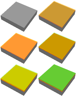 Then, a process called photolithography is used to create multiple layers on the wafer. Ultra violet light is shot on a patterned mask, or a stencil, which then only lights a specific patter shine onto the wafer. The stencil protects certain areas from the ultra violet light. 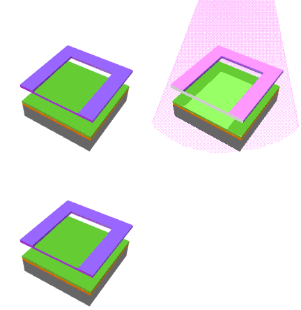 The exposed areas are chemically changed from the light and soften. Then the soft areas are dissolved away in a solution. This reveals a pattern on the wafer that was created by the mask. 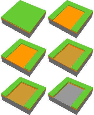 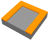 Next, the silicon dioxide is washed away with more chemicals, leaving a pattern of silicon dioxide on the wafer. Below is a picture of what is left after the excess materials are dissolved away. Then the process is repeated to create another layer. Another thin layer of silicon dioxide is grown over the previous pattern and the wafer. Then a layer of polysilicon and another layer of Photoresist are applied to the wafer. 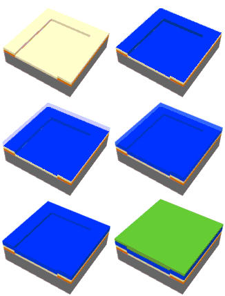 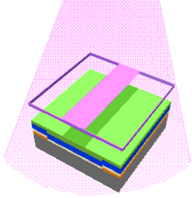 Ultraviolet light is then shined on another mask, which lets only another specific pattern of light through. The exposed Photoresist areas are then washed away with chemicals. Then the Photoresist that is left is removed, leaving a layer of polysilicon and the first layer of silicon dioxide. 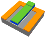 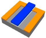 |
||
|
| |||
|---|---|---|---|