 |
|
|
|
In the Forums... |
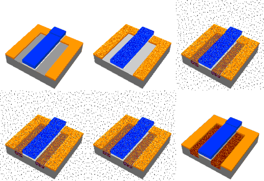
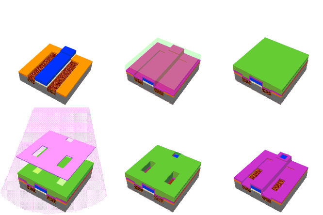
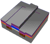
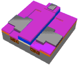
Posted: November 22, 2000 Written by: Tuan "Solace" Nguyen Ion Doping  This is the process of sniffing ions to get high. Just kidding. After the silicon dioxide layer and the polysilicon layer is created, the wafer then goes through a process called "Ion Implantation", which is also called doping. The exposed areas of the wafer (parts shown in gray) are bombarded with different chemical impurities called ions. These ions are implanted into the silicon wafer to change the way the silicon in the implanted areas conduct electricity. Ring Around the Rosy This entire process is repeated until “windows” or openings are created in the patterns on the waver. These openings enable connections to be made between layers.  After this is completed, atoms of metal are coated onto the wafer, filling the little openings. Then another layering process leaves stripes of metal that make the electrical connections on the processor die. This is where manufacturers use different types of metals like aluminum and/or copper.   This layer is called an "Interconnect". This is what you may have been hearing for the past few months with Intel and AMD switching from aluminum interconnects to copper ones. Copper conducts electricity better than aluminum, therefore enabling faster processors in the coming future. About twenty or so layers are connected to form the processors circuitry in a 3D structure. The number of layers depends on the processor’s design. |
||
|
| |||
|---|---|---|---|