How CPUs Are Made
Posted: November 22, 2000
Written by: Tuan "Solace" Nguyen
Introduction
It’s that time of the week again, when I’m just itching to find out how something works. It just bothers me when I don’t know how something functions, especially when I use that thing everyday of my life. I’m talking about a processor, a CPU, a chip. How exactly is it made? Of course I already know how, that’s why I’m writing this guide, but perhaps you don’t. Let’s get on with the show.
Potato Chips
Every component inside your computer has some type of IC (integrated circuit) chip on it. And each chip is made with the same design principles in mind. These chips contain a small silicon die inside them, which contain thousands to millions of transistors.
Transistors
What is a transistor? Transistors are miniature electronic switches. They are the building blocks of a microprocessor, which is the brain of the computer. You can think of a transistor like it was a light switch. They have two operating positions, on and off. This on and off, or binary functionality of transistors enables the processing of information in a computer. This is why binary numbers are based on 1’s (on) and 0’s (off).

At their most basic level, transistors may seem simple. But their development actually required many years of painstaking research. Before transistors, computers relied on slow, inefficient vacuum tubes and mechanical switches to process information. In 1958, engineers (one of them being Intel founder Robert Noyce) managed to put two transistors onto a silicon crystal and create the first integrated circuit, that led to the microprocessor.
The only information computers understand are electrical signals that are switched on and off. To comprehend transistors, it is necessary to have an understanding of how a switched electronic circuit works.
Switched electronic circuits consist of several parts. One is the circuit pathway where the electrical current flows - typically through a wire. Another is the switch, a device that starts and stops the flow of electrical current by either completing or breaking the circuit's pathway. If you cut a wire, the flow will stop, and if you reconnect the ends, the flow continues. So in essence, you can be a human transistor.
Transistors have no moving parts and are turned on and off only by electrical signals. The on/off switching of transistors facilitates the work performed by microprocessors. Something that has only two states (on or off), like a transistor, can be referred to as binary. The transistor's on state is represented by a 1 and the off state is represented by a 0. Specific sequences and patterns of 1s and 0s generated by multiple transistors can represent letters, numbers, colors and graphics. This is known as binary notation.

For example, 1 in decimal would be 1 in binary. 2 would be 10. 3 would be 11. 4 would be 100. 5 would be 101. 6 would be 110. 7 would be 111. And so on. Here’s “Tweak3D” written in binary:
T 0101 0100
W 0101 0111
E 0100 0101
A 0100 0001
K 0100 1011
3 0000 0011
D 0100 0100
Letters are represented by ASCII in this example. E.g. "T" is the ASCII equivalent of 01010100 (binary), or 84 (decimal). Interesting, huh? Maybe I should type out this entire article in binary. What fun! So how exactly does a transistor work inside a processor? Let’s take a look.
Transistors @ Work
Adding certain types of impurities or other materials to the silicon in a transistor changes its crystalline structure and enables it to conduct electricity. Silicon containing boron is called p-type silicon - p for positive or having no electrons. Silicon containing phosphorus is called n-type silicon - n for negative or having electrons.
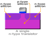
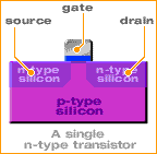
Transistors consist of three terminals -- the source, the gate and the drain. In the n-type transistor, both the source and the drain are negatively charged and sit on positively charged p-silicon. When positive voltage is applied to the gate, electrons in the p-silicon are attracted to the area under the gate forming an electron channel between the source and the drain. When positive voltage is applied to the drain, the electrons are pulled from the source to the drain. In this state the transistor is on and there is electrical flow. If the voltage at the gate is removed, electrons aren't attracted to the area between the source and drain anymore and the pathway is broken and the transistor is turned off.
Well, now that you know how a transistor works let’s get to the real deal.
Getting Real Clean
The Clean Room
The clean room is a room where there are virtually zero dust particles. Class 1 clean rooms are the cleanest of all with only 1 speck of dust per cubic foot. Inside clean rooms is where you can find raw processors, without their packaging. One small speck of dust could damage thousands of transistors on a processor rendering it useless.
Clean rooms are 10,000 times cleaner than a hospital operating room. There are sophisticated air filtering systems which purify the air once every 10 minutes to keep the room incredibly clean. But keeping the room clean and having people entering in and out all the time is likely going to be disastrous. This is why the engineers that work inside a clean room must wear a clean suit or what Intel calls a bunny suit. It’s almost like working for the CDC (Center for Disease and Control). The suits are made out of special non-linting and non-static material that you wear over your everyday clothing.

Above is a picture of a tiny grain of salt that has damaged thousands of transistors on a microchip. If the city of New York was a processor die, then that grain of salt would be a football stadium slammed into the streets from nowhere. Imagine the damage that would cause.

Above is a picture of Intel engineers preparing to enter the clean room.
How a Processor is Made
Processors are mainly made from silicon. Silicon is extracted from minerals in the earth and purified to remove impurities and other dust and particles. Sand on beach also contains large amounts of silicon.
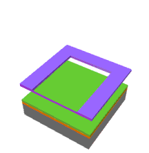
The purified silicon is then melted and made into a long solid cylinder of silicon, called an ingot, ready to be cut into thin slices called wafers. Then each silicon wafer is buffed and polished into a virtually featureless surface. This is necessary in order to manufacture chips on the wafer.
Fabrication and Layering
One silicon wafer can be used to manufacture many processors, called dies. A single wafer can contain a hundred or more processor dies.
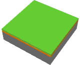
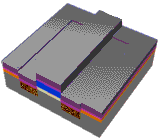
The first layer of silicon dioxide is grown by exposing it to extreme heat and gases. This growth is similar to how rust grows on metal when exposed to moisture. Rust however, grows very slowly over time. The silicon dioxide grows much faster and creates an extremely thin layer of material on the wafer. Then the wafer is coated with a chemical called Photoresist. Photoresist becomes soluble, meaning it can be dissolved away, when exposed to ultraviolet light.
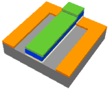
Then, a process called photolithography is used to create multiple layers on the wafer. Ultra violet light is shot on a patterned mask, or a stencil, which then only lights a specific patter shine onto the wafer. The stencil protects certain areas from the ultra violet light.
The exposed areas are chemically changed from the light and soften. Then the soft areas are dissolved away in a solution. This reveals a pattern on the wafer that was created by the mask.
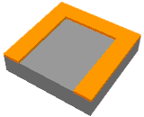
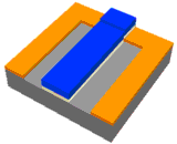
Next, the silicon dioxide is washed away with more chemicals, leaving a pattern of silicon dioxide on the wafer. Below is a picture of what is left after the excess materials are dissolved away. Then the process is repeated to create another layer. Another thin layer of silicon dioxide is grown over the previous pattern and the wafer. Then a layer of polysilicon and another layer of Photoresist are applied to the wafer.
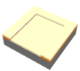
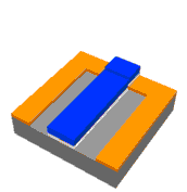
Ultraviolet light is then shined on another mask, which lets only another specific pattern of light through. The exposed Photoresist areas are then washed away with chemicals. Then the Photoresist that is left is removed, leaving a layer of polysilicon and the first layer of silicon dioxide.
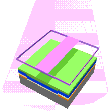
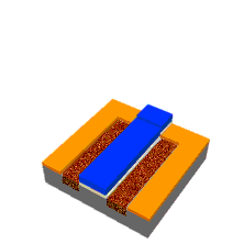
Ion Doping
This is the process of sniffing ions to get high. Just kidding. After the silicon dioxide layer and the polysilicon layer is created, the wafer then goes through a process called "Ion Implantation", which is also called doping. The exposed areas of the wafer (parts shown in gray) are bombarded with different chemical impurities called ions. These ions are implanted into the silicon wafer to change the way the silicon in the implanted areas conduct electricity.
Ring Around the Rosy
This entire process is repeated until “windows” or openings are created in the patterns on the waver. These openings enable connections to be made between layers.
After this is completed, atoms of metal are coated onto the wafer, filling the little openings. Then another layering process leaves stripes of metal that make the electrical connections on the processor die. This is where manufacturers use different types of metals like aluminum and/or copper.
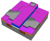
This layer is called an "Interconnect". This is what you may have been hearing for the past few months with Intel and AMD switching from aluminum interconnects to copper ones. Copper conducts electricity better than aluminum, therefore enabling faster processors in the coming future. About twenty or so layers are connected to form the processors circuitry in a 3D structure. The number of layers depends on the processor’s design.
The Cutting Edge

These are just a few of the more than 250 steps in making a processor or any other type of chip. After the processors have been completely manufactured on the silicon wafer, each processor die is tested, and if everything is okay, the dies are cut from the wafer using a diamond saw. Each processor core is then inserted into a protective packaging -- your typical ceramic plate -- and is connected using thin gold wires to the packaging where electrical traces lead to pins, which are located externally.
Each processor is tested one more time to ensure that everything is working properly and then it is time for it to see the day of light.
Conclusion
What I’ve just explained to you are just some basic concepts and information behind how a processor is made. The design of a processor takes years, and the manufacturing part isn’t even half the work. Designing a processor takes hundreds and thousands of people, and millions of man-hours and dedicated hard work. Also, you need a sophisticated fabrication facility, which costs big bucks. We’re talking around 5 billion dollars per fabrication plant. Intel builds a new fabrication plant every 5 years. That alone tells you the costs of manufacturing -- let alone design.
Next time you go out and purchase a CPU upgrade and wonder why in the world it costs so much, think back to this article here, and you’ll see where most of the money you spend goes.
I hope you’ve learned a little more about what goes into making your computer and how it works. I’ll talk about other devices next time but the processor is the most sophisticated and delicate device in your computer, or any other computer for that matter. If you haven’t done so, take a look at some of the other How It Works guides I’ve written here.
Once again, thanks for reading. Feel free to write me with comments and or questions here or visit me and other Tweak3D members in channel #tweak3d on any Undernet server, IRC.
Want to return to the normal guide? Click here!
All Content Copyright ©Dan Kennedy; 1998-2000